Digital Design · Computer Architecture
Verilog Vesp1.0 CPU Implementation
1 / 2
Overview
The VESP1.0 is a 16-bit CPU architecture designed by Yavuz Oruc. It uses an accumulator-based architecture with a 16-bit word length and a 12-bit memory address space.
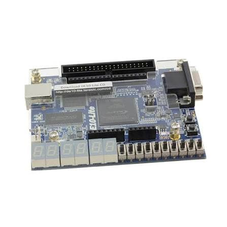
I implemented the VESP1.0 processor in Verilog, modeling the processor's datapath and control logic as a finite state machine. The implementation includes the CPU registers, instruction decoding, arithmetic and logical operations, memory access, conditional branching, and processor control.
The processor uses five main register groups: the 16-bit accumulator (A), 16-bit operand register (B), 12-bit memory address register (MAR), 16-bit instruction register (IR), and 13-bit program counter (PC). It also maintains Zero, Sign, Carry, and Overflow flags for ALU operations.
Design Approach
Processor Registers
- —A (Accumulator): 16-bit register that stores operands and results of arithmetic and logical operations
- —B (Operand Register): 16-bit register used to hold the secondary operand for ALU operations
- —MAR (Memory Address Register): 12-bit register that stores the address of the current instruction or data location
- —IR (Instruction Register): 16-bit register that stores the instruction currently being executed
- —PC (Program Counter): 13-bit register that points to the next instruction to execute
- —Flags: Zero, Sign, Carry, and Overflow status bits updated by ALU operations
Instruction Set
- —ADD (000): Adds the contents of A and B and stores the result in A
- —CMP (001): Complements the contents of A
- —LDA (010): Loads a value from memory into the processor
- —MOV (011): Moves a value using indirect memory addressing
- —JMP (100): Unconditionally jumps to the address specified by the instruction
- —JEZ (101): Jumps when the accumulator contains zero
- —JPS (110): Jumps when the accumulator contains a positive value
- —HLT (111): Halts processor execution
Control Architecture
- —Implemented the processor control logic as a finite state machine
- —Fetch state reads the instruction at the address stored in the PC and loads it into the IR
- —The PC is incremented during instruction fetch
- —Decode logic determines the operation from the instruction opcode
- —Execute states perform the required ALU, memory, or control-flow operation
- —Processor flags are updated based on the results of applicable ALU operations
Simulation & Testing
I verified the Verilog implementation through simulation using a test program that adds two numbers and stores the resulting value in the accumulator register.
The simulation allowed the processor's instruction execution and register updates to be observed across multiple clock cycles, verifying the behavior of the implemented datapath and control logic.
Key Features
- —16-bit accumulator-based CPU architecture
- —Verilog RTL implementation
- —Finite state machine control logic
- —8-instruction instruction set
- —16-bit accumulator and operand registers
- —12-bit memory addressing
- —13-bit program counter
- —Zero, Sign, Carry, and Overflow flags
- —Arithmetic, memory access, and conditional branching instructions
- —Simulation-based verification using an addition test program
- Verilog
- Digital Design
- Computer Architecture
- Finite State Machines
- Instruction Set Architecture
- Simulation